General Description
The Evaluation Board demonstrates the RT4539 device provides a highly integrated white LED driver solution for notebook and Tablet LCD backlight. The device is a white-LED driver featuring a 36V high efficiency asynchronous boost converter and six 35mA high precision current sinks with a maximum of ±2% current mismatching for excellent brightness uniformity in each string of LEDs. The RT4539 has five dimming modes including DC mode, direct PWM mode, PWM-26k mode, mix mode and mix-26k mode that can be controlled by PWM signal or an I2C master, or both. In addition, The RT4539 has a wide input voltage operating range from 2.7V to 24V and contains I2C interface for controlling the dimming mode, operating frequency, LED current slope time and the LED current. It is suitable for single/two cell battery input to drive LED light bars which contain six strings in parallel.
Performance Specification Summary
Summary of the RT4539WSC Evaluation Board performance specification is provided in Table 1. The ambient temperature is 25°C.
Table 1. RT4539WSC Evaluation Board Performance Specification Summary
|
Specification
|
Test Conditions
|
Min
|
Typ
|
Max
|
Unit
|
|
Input Voltage Range
|
|
2.7
|
3.8
|
24
|
V
|
|
Operation Frequency
|
Boost operates at PWM mode default = 600kHz@0x07h
|
300
|
600
|
1600
|
kHz
|
|
Switching Frequency Accuracy
|
Boost operates at PWM mode, fSW = 600kHz
|
-10
|
--
|
10
|
%
|
|
Switching Current Limitation
|
|
2
|
2.5
|
3
|
A
|
|
Maximum LED Current Setting
|
LED 100% setting, register address = ”02h”,
Step = 0.12mA
|
10.04
|
--
|
35
|
mA
|
|
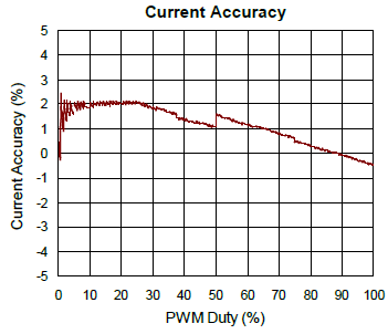
LED Current Accuracy
|
PWM duty = 100%, IFBx = 20mA,
PWM frequency = 1kHz
|
-3
|
--
|
3
|
%
|
|
PWM duty = 5%, IFBx = 20mA,
PWM frequency = 1kHz
|
-5
|
--
|
5
|
|
PWM duty = 1%, IFBx = 20mA,
PWM frequency = 1kHz
|
-15
|
--
|
15
|
|
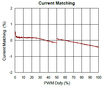
LED Current Matching
|
PWM duty = 100%, IFBx = 20mA,
PWM frequency = 1kHz
|
-2
|
--
|
2
|
%
|
|
PWM duty = 5%, IFBx = 20mA,
PWM frequency = 1kHz
|
-5
|
--
|
5
|
|
PWM duty = 1%, IFBx = 20mA,
PWM frequency = 1kHz
|
-10
|
--
|
10
|
Power-up Procedure
Suggestion Required Equipments
- RT4539WSC Evaluation Board
- DC power supply capable of at least 30V and 4A
- DC power supply capable of at least 6V and 1A
- Function Generator
- Oscilloscope
- LED Light Bar
Quick Start Procedures
The Evaluation Board is fully assembled and tested. Follow the steps below to verify board operation. Do not turn on supplies until all connections are made.
Proper measurement equipment setup and follow the procedure below.
1) With power off, connect the input power supply to VIN and GND pins.
2) With power off, connect the input power supply to EN and GND pins.
3) With power off, connect the function generator to PWM and GND pins.
4) With power off, connect LED light bar to Vout and FB1 to FB6 pins.
5) Turn on the power supply at the input.
6) Once the proper output voltage is established, adjust the brightness within the operating ranges and observe the FB1 to FB6 current, switching frequency and other performance.
Detailed Description of Hardware
Headers Description and Placement
Carefully inspect all the components used in the EVB according to the following Bill of Materials table, and then make sure all the components are undamaged and correctly installed. If there is any missing or damaged component, which may occur during transportation, please contact our distributors or e-mail us at evb_service@richtek.com.
Test Points
The EVB is provided with the test points and pin names listed in the table below.
|
Test Point/
Pin Name
|
Function
|
|
LX
|
Switch node of boost converter.
|
|
PGND
|
Power ground.
|
|
SDA
|
Data signal input of I2C interface.
|
|
SCL
|
Clock signal input of I2C interface.
|
|
PWM
|
PWM dimming control input.
|
|
EN
|
Enable control input (active high).
|
|
VIN
|
Device power supply input.
|
|
VOUT
|
Output of boost converter.
|
|
VCP
|
Internal LDO output pin. Connect a capacitor (Ccp) between this pin and the ground reference.
|
|
FB1
|
Current sink for LED1.
|
|
FB2
|
Current sink for LED2.
|
|
FB3
|
Current sink for LED3.
|
|
FB4
|
Current sink for LED4.
|
|
FB5
|
Current sink for LED5.
|
|
FB6
|
Current sink for LED6.
|
Bill of Materials
|
VIN = 3.8V, EN = 3.3V, fSW = 600kHz, ILEDmax = 20mA/Ch
|
|
Reference
|
Count
|
Part Number
|
Value
|
Description
|
Package
|
Manufacturer
|
|
U1
|
1
|
RT4539WSC
|
RT4539WSC
|
Boost Converter with 6-CH LED Driver
|
WL-CSP-20B 1.71x2.371 (BSC)
|
RICHTEK
|
|
C1, C10
|
2
|
UMK316AB7475KL-T
|
4.7µF
|
Capacitor, Ceramic, 50V, X7R
|
1206
|
TAIYO YUDEN
|
|
C3, C8
|
2
|
00805B105K500CT
|
1µF
|
Capacitor, Ceramic, 50V, X7R
|
0805
|
WALSIN
|
|
C4, C5
|
2
|
UMK316BJ225KD-T
|
2.2µF
|
Capacitor, Ceramic, 50V, X5R
|
1206
|
TAIYO YUDEN
|
|
C13
|
1
|
0603X105K250CT
|
1µF
|
Capacitor, Ceramic, 25V, X7R
|
0603
|
WALSIN
|
|
D1
|
1
|
SR26
|
SR26
|
SR26
|
SMA/DO-214AC
|
PANJIT
|
|
L2
|
1
|
NR8040T068M
|
6.8µH
|
6.8µH
|
L-8x8
|
TAIYO YUDEN
|
|
R3
|
1
|
WR06X10R0FTL
|
10
|
10
|
0603
|
WALSIN
|
|
R5, R6
|
2
|
RTT034701FTP
|
4.7k
|
4.7k
|
0603
|
WALSIN
|
|
R7, R8
|
2
|
RTT031001FTP
|
1k
|
1k
|
0603
|
WALSIN
|
Typical Applications
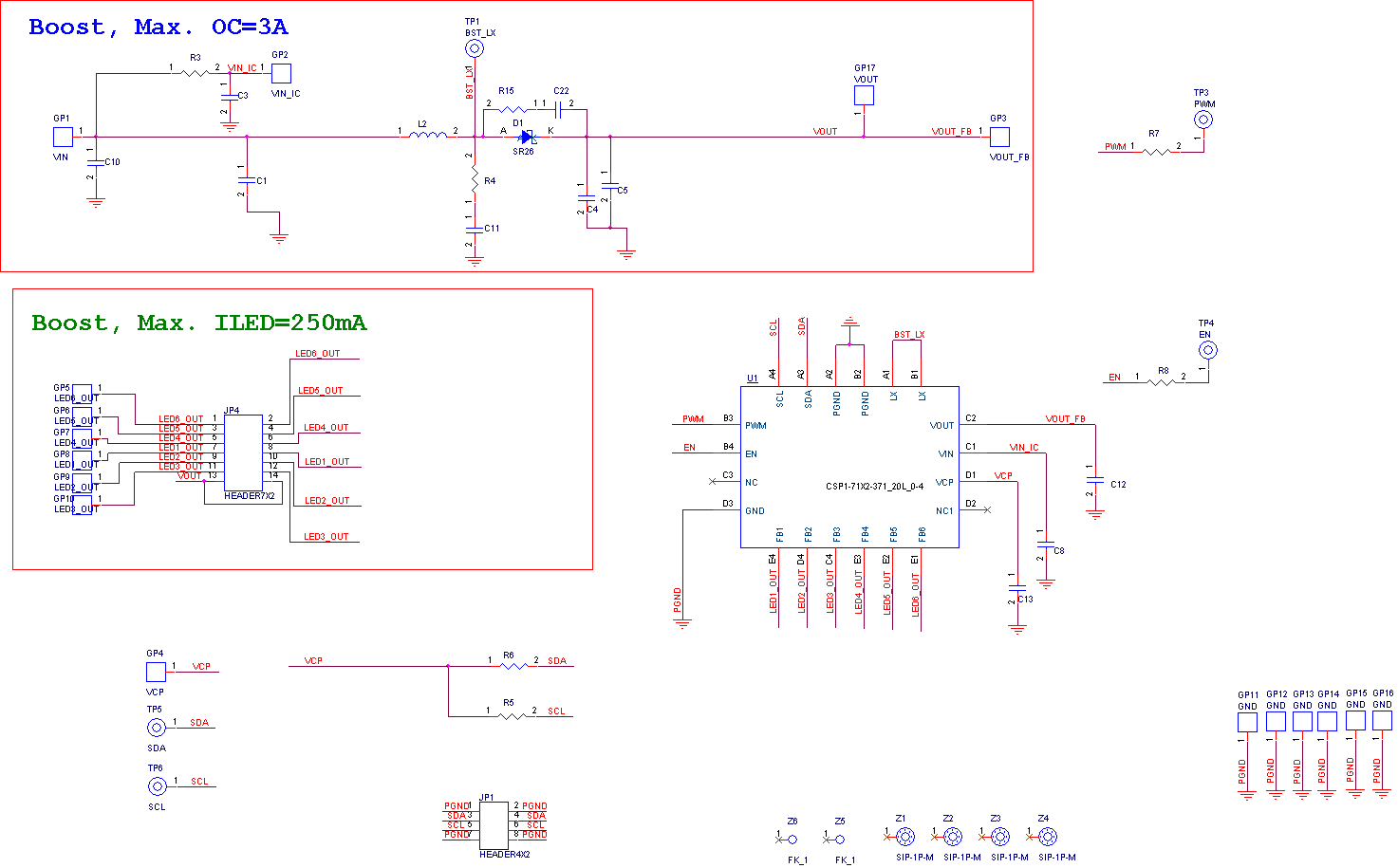
EVB Schematic Diagram
Measure Result
|
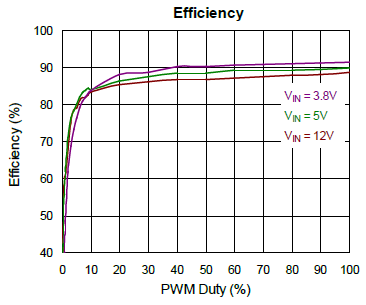
Efficiency Measurement
|
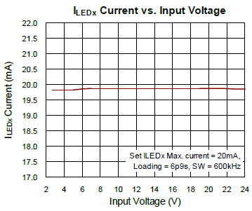
LED Current Measurement
|
|
|
|
|
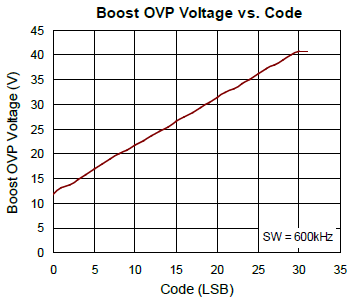
OVP Threshold Voltage vs. Input Voltage
|
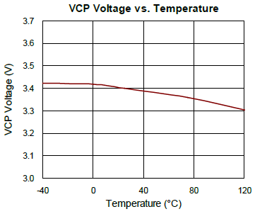
VDC Voltage vs. Temperature
|
|
|
|
|
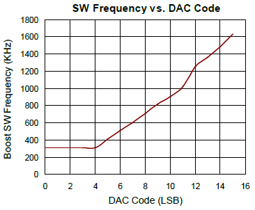
Switching Frequency vs. I2C Code
|
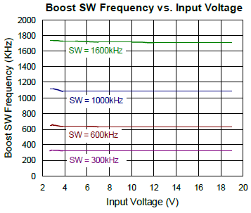
Switching Frequency vs. Input Voltage
|
|
|
|
|
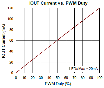
Efficiency vs. Output Current
|
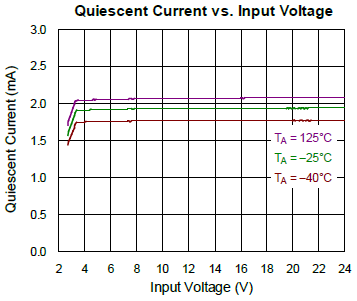
Question Current vs. Input Voltage
|
|
|
|
|
Output Voltage vs. Input Voltage
|
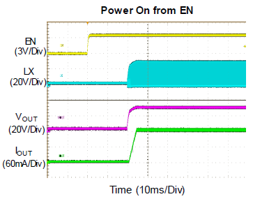
Power-On from EN
|
|
|
|
|
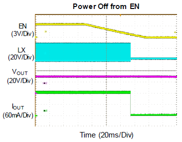
Power-Off from EN
|
Accuracy
|
|
|
|
|
Matching
|
|
|
|
|
Evaluation Board Layout
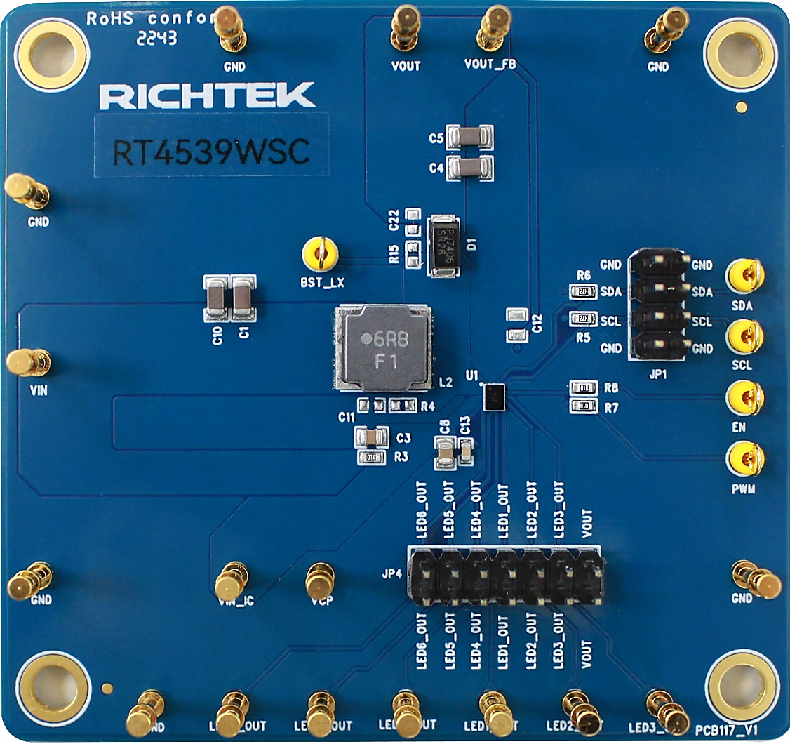
Figure 1 to Figure 4 are RT4539WSC Evaluation Board layout. This board size is 75mm x 70mm and is constructed on four-layer PCB, outer layers with 1 oz. Cu and inner layers with 1 oz. Cu.
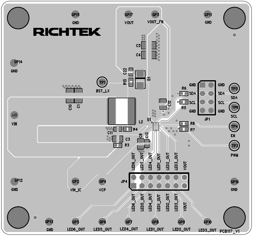
Figure 1. Top View (1st layer)
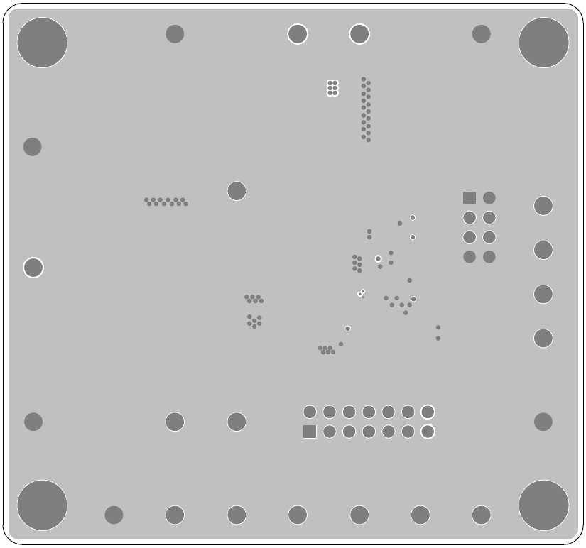
Figure 2. PCB Layout—Inner Side (2nd Layer)
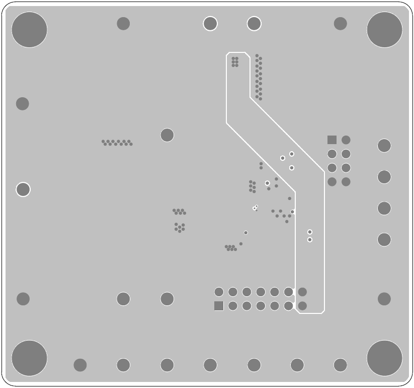
Figure 3. PCB Layout—Inner Side (3rd Layer)
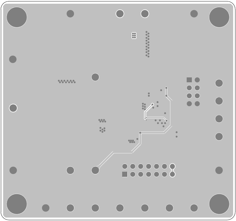
Figure 4. Bottom View (4th Layer)